Silicon carbide photovoltaic cells

The symmetric samples and solar cells were fabricated with Czochralski grown n-type double-side textured, 170-µm-thick, 1 Ω cm silicon <100> wafers produced by LONGi. The wafers were cleaned i.
Contact online >>

Performance analysis of cubic silicon carbide solar cell as an

In this research article, a 3C–SiC-based single-junction solar cell is evaluated using a two-dimensional finite element method. Effects of n + and p + thicknesses and operating temperature on the performance of n + pp + 3C–SiC solar cell are simulated to find its real efficiency. For a cell with a thickness of 5 µm, the efficiencies of 12.52%, 11.2%, 10.3%, and 8.8% are obtained for n

Review of silicon recovery in the photovoltaic industry

Figure 1 illustrates the value chain of the silicon photovoltaic industry, ranging from industrial silicon through polysilicon, monocrystalline silicon, silicon wafer cutting, solar cell production, and finally photovoltaic (PV) module assembly. The process of silicon production is lengthy and energy consuming, requiring 11–13 million kWh/t from industrial silicon to

Titanium-carbide MXenes for work function and interface

This opens up new opportunities for MXene applications in optoelectronics and in particular in photovoltaics, where some initial studies have already been presented for organic solar cells 36, Si

Crystal structures and the electronic properties of silicon-rich

Si-rich-silicon carbide Photovoltaic Density functional theory ABSTRACT Silicon carbide has been used in a variety of applications including solar cells due to its high stability. The high bandgap of pristine SiC, necessitates nonstoichiometric silicon carbide materials to be considered to tune the band gap for efficient solar light absorptions.

Silicon Carbide (SiC) Boosts Solar Inverter System Efficiency

There are three primary inverter architectures: micro PV inverter, PV string inverter and PV central inverter. This article will look at these architectures and how SiC fits into the picture. Silicon carbide technology: A long history, new for today. Scientists first synthesized SiC in 1891. SiC occurs naturally, though it is rare on Earth.

Can crystalline silicon (c-Si) solar cells have a transparent passivating contact?

A highly transparent passivating contact (TPC) as front contact for crystalline silicon (c-Si) solar cells could in principle combine high conductivity, excellent surface passivation and high optical transparency. However, the simultaneous optimization of these features remains challenging.

Are passivating contacts a viable solution for silicon solar cells?

Passivating contacts hold promise for silicon solar cells yet the simultaneous optimization of conductivity, defect passivation and optical transparency remains challenging. Now Köhler et al. devise a passivating contact based on a double layer of nanocrystalline silicon carbide that overcomes these trade-offs.

Hybrid photovoltaic solar system performance enriched by

Increases in solar cell temperature significantly impact photovoltaic output power, reducing it by approximately 0.8% for every temperature rise. The silicon carbide-based porous materials are chosen for this investigation and offer better thermal conductivity, better thermal stability, and specific porous dimension of 400 mm × 330 mm ×

Silicon heterojunction solar cells with up to 26.81% efficiency

The total series resistance of the solar cell is reduced from the original 0.37 to 0.2 Ω cm 2, yielding a record FF for single-junction silicon solar cell. Methods Solar cell fabrication

Silicon Carbide in Solar Energy

SiC is used in power electronics devices, like inverters, which deliver energy from photovoltaic (PV) arrays to the electric grid, and other applications, like heat exchangers in concentrating solar power (CSP) plants and electric vehicles.

Amorphous silicon carbide passivating layers for crystalline-silicon

Very efficient crystalline silicon (c-Si) solar cells can be obtained when thin intrinsic and doped hydrogenated amorphous silicon (a-Si:H) layers are used for passivation and carrier selectivity. 1,2 A well known loss mechanism of such a-Si:H/c-Si heterojunction devices is parasitic absorption of blue light in the a-Si:H layers on the light-entering side. 3–6 Several

Semi-transparent silicon-rich silicon carbide photovoltaic solar

All silicon-rich silicon carbide (Si-rich SixC1−x)-based single p–i–n junction photovoltaic solar cells (PVSCs) were fabricated by growing nonstoichiometric Si-rich SixC1−x

Silicon carbide passivating contact for 24%-efficient crystalline

A European research team led by Germany''s Forschungszentrum Jülich has developed a 24%-efficient crystalline silicon solar cell with a highly transparent passivating contact based on silicon carbide.

Transparent silicon carbide/tunnel SiO2 passivation for c‐Si solar cell

N-type microcrystalline silicon carbide (μc-SiC:H(n)) is a wide bandgap material that is very promising for the use on the front side of crystalline silicon (c-Si) solar cells. which corresponds to cheap low-quality wafer, the solar cell parameters are smaller. For an IBC solar cell with (ii) the MgF 2 /μc-SiC:H(n) ARC front side, this

What is a passivated rear contact for n-type silicon solar cells?

A passivated rear contact for high efficiency n-type silicon solar cells enabling high V oc s and FF > 82%. In Proc. 28th European Photovoltaic Solar Energy Conference and Exhibition (2013). Feldmann, F. et al. Tunnel oxide passivated contacts as an alternative to partial rear contacts. Sol. Energy Mater. Sol. Cells 131, 46–50 (2014).

Cubic Silicon Carbide (3C–SiC) as a buffer layer for high efficiency

1. Introduction. The relentless effort towards developing a viable photovoltaic (PV) solar cell technology that can substitute conventional fossil fuel has led to the discovery of group II-IV compound chalcogenides, which can be used in solar cells to replicate the similar efficiency achieved conventionally [1].Among these, Cadmium Telluride (CdTe) compound

Amorphous silicon

Amorphous silicon (a-Si) is the non-crystalline form of silicon used for solar cells and thin-film transistors in LCDs.. Used as semiconductor material for a-Si solar cells, or thin-film silicon solar cells, it is deposited in thin films onto a variety of flexible substrates, such as glass, metal and plastic. Amorphous silicon cells generally feature low efficiency.

Silicon Carbide (SiC) Boosts Solar Inverter System

There are three primary inverter architectures: micro PV inverter, PV string inverter and PV central inverter. This article will look at these architectures and how SiC fits into the picture. Silicon carbide technology: A

Blistering-free polycrystalline silicon carbide films for double-sided

In this work, we present a study of PECVD preparation of B-doped polycrystalline silicon carbide (poly-SiC x) films with a blistering-free appearance by incorporating carbon (C)

Socio-Economic and Environmental Impacts of Silicon Based Photovoltaic

Some of them are pulling methods (EFG and String-Ribbon), tearing with a thin layer of silver and using laser. 1.1.2. Total energy expenditure for solar cell manufacturing The total energy expenditure for solar cell manufacturing is the sum of the aforementioned processes. Mono-crystalline cells require up to 1000 kWh/kg-Si.

Blistering-free polycrystalline silicon carbide films for double-sided

Passivating contacts featuring a polysilicon (poly-Si) and ultrathin silicon oxide (SiO x) stack on monocrystalline silicon (c-Si) as the key component for tunnel oxide passivating contact (TOPCon) [1], POLO [2] and SIPOS [3] technologies, have attracted considerable attentions in the c-Si photovoltaic (PV) community eliminating the direct contact of Si

What is the conversion efficiency of crystalline silicon heterojunction solar cells?

Masuko, K. et al. Achievement of more than 25% conversion efficiency with crystalline silicon heterojunction solar cell. IEEE J. Photovolt. 4, 1433–1435 (2014). Glunz, S. W. et al. The irresistible charm of a simple current flow pattern – 25% with a solar cell featuring a full-area back contact.

Material Properties of Nanocrystalline Silicon Carbide for

[1, 4] For silicon carbide, many attempts have been made to integrate it into various types of solar cell structures, [5-9] but the best results were achieved using a low-temperature approach by a wet-chemically grown silicon oxide in combination with two different nanocrystalline silicon carbide layers, one passivating and one conducting layer.

Low-Temperature Growth of Hydrogenated Amorphous Silicon Carbide Solar

Up to date, dye-sensitized solar cell (DSSC), perovskite solar cell and hydrogenated amorphous silicon (a-Si:H) thin film solar cell, which have all light absorption windows of 300 nm to 800 nm

The Importance of New "Sand-to-Silicon

The photovoltaic industry initiated with monocryst. silicon and multicryst. silicon solar cell having conversion efficiency reached up to approx. 22.9% and 20.8%, resp. High-purity silicon carbide and two different high-purity hydrothermal quartzes were charged as raw materials at different molar ratios. The charge was in the form of lumps

Silicon solar cells: materials, technologies, architectures

The thin-film silicon solar cell technology is based on a versatile set of materials and alloys, in both amorphous and microcrystalline form, grown from precursor gases by PECVD. Amorphous silicon carbide passivating layers for crystalline-silicon-based heterojunction solar cells. J. Appl. Phys., 118 (2015), p. 065704. View in Scopus Google

Light and elevated temperature induced degradation and

The fast-firing step commonly applied at the end of solar cell production lines is known to trigger light-induced degradation effects on solar cells made on different silicon materials. In this

Diamond Wire Sawing of Solar Silicon Wafers: A Sustainable

The wafers are cut from silicon ingots using the wire sawing process (see Figure 1), which is an expensive step in the solar cell manufacturing process. Recent industry trends indicate a shift from the loose abrasive slurry (LAS) sawing to fixed abrasive diamond wire sawing (DWS) process for slicing silicon wafers [2, 3].

Can crystalline silicon solar cells have junctions without diffused emitters?

Device designs that avoid diffused emitter regions and direct metal-absorber contacts, commonly denoted as passivated contacts, are key enablers for a further increase of efficiency. So far, three concepts have been developed that enable junction formation in crystalline silicon solar cells without diffused emitters.

Heterojunction Amorphous Silicon Solar Cells with n-Type

n-Type Microcrystalline Cubic Silicon Carbide as a Window Layer To cite this article: Shunsuke Ogawa et al 2007 Jpn. J. Appl. Phys. 46 518 in a tandem-type solar cell combined with amorphous silicon (a-Si:H) and microcrystalline silicon (mc-Si:H) thin-film solar cells.1) In the fabrication of a-Si:H-based thin-film solar

Photogenerated Carrier Transport Properties in Silicon Photovoltaics

Electrical transport parameters for active layers in silicon (Si) wafer solar cells are determined from free carrier optical absorption using non-contacting optical Hall effect measurements.

Silicon carbide passivating contact for 24%-efficient crystalline

A European research team led by Germany''s Forschungszentrum Jülich has developed a 24%-efficient crystalline silicon solar cell with a highly transparent passivating

About Silicon carbide photovoltaic cells

About Silicon carbide photovoltaic cells

The symmetric samples and solar cells were fabricated with Czochralski grown n-type double-side textured, 170-µm-thick, 1 Ω cm silicon <100> wafers produced by LONGi. The wafers were cleaned i.

To be able to judge which HWCVD deposition parameter has a significant influence on.

The passivation quality of the layer was tested on symmetric samples and solar cells before ITO deposition by measuring the photo-conductance of the wafer using a Sinton WC.

The SIMS (time-of-flight-SIMS IV by IONTOF) measurement was conducted to analyse the interface properties of the nc-SiC:H(n)/SiO2/c-Si(n) stack, to investigate the correlat.

The high-resolution bright-field STEM images were obtained with a probe aberration corrected Hitach HF5000 microscope. EDX mapping of the O-K edge, Si-L.

The UPS system is a MULTIPROBE MXPS system from Scienta Omicron with an ARGUS hemispherical electron spectrometer and part of the JOSEPH cluster syst.To date, the use of 3C-SiC for photovoltaics has not been considered due to the band gap of 2.3 eV being too large for conventional solar cells. Doping of 3C-SiC with boron introduces an energy level of 0.7 eV above the valence band. Such energy level may form an intermediate band (IB) in the band gap.

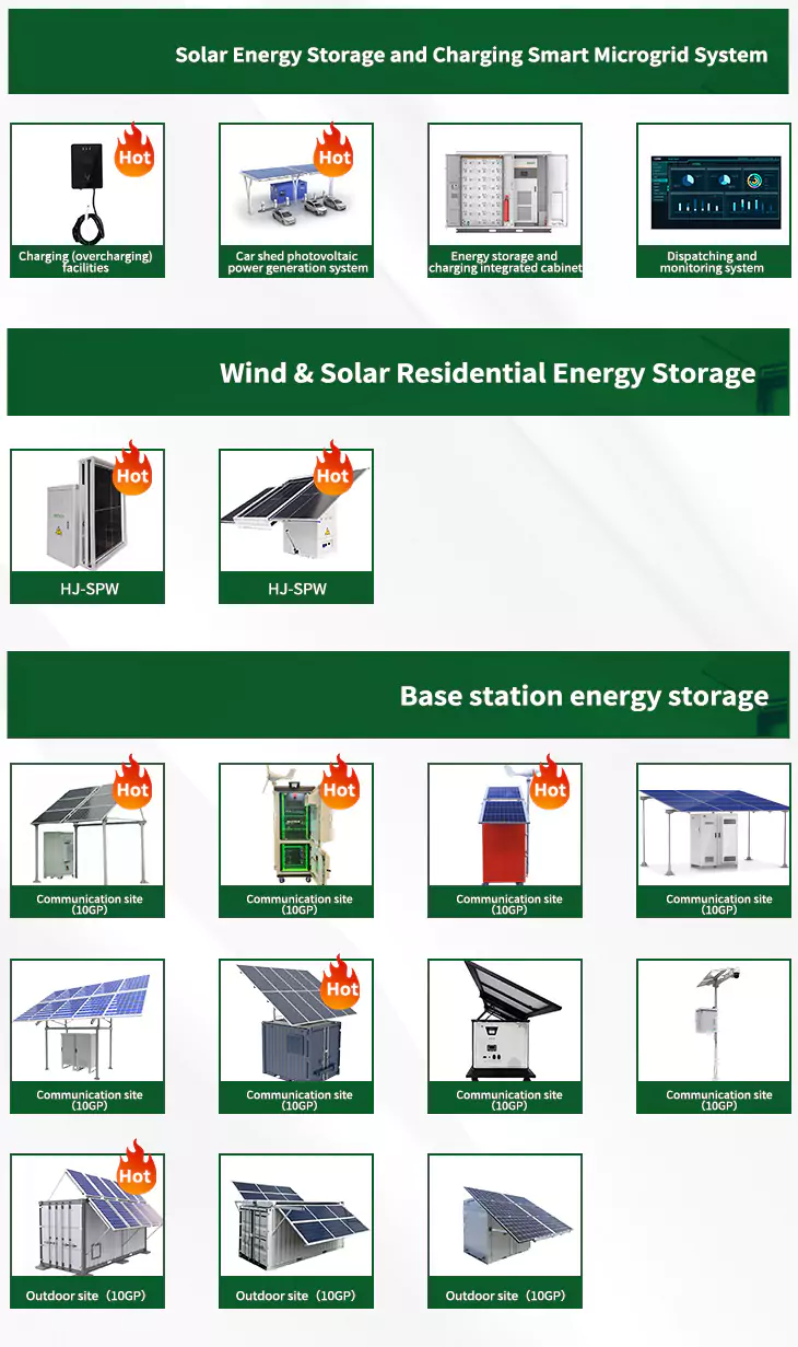
As the photovoltaic (PV) industry continues to evolve, advancements in Silicon carbide photovoltaic cells have become critical to optimizing the utilization of renewable energy sources. From innovative battery technologies to intelligent energy management systems, these solutions are transforming the way we store and distribute solar-generated electricity.

When you're looking for the latest and most efficient Silicon carbide photovoltaic cells for your PV project, our website offers a comprehensive selection of cutting-edge products designed to meet your specific requirements. Whether you're a renewable energy developer, utility company, or commercial enterprise looking to reduce your carbon footprint, we have the solutions to help you harness the full potential of solar energy.

By interacting with our online customer service, you'll gain a deep understanding of the various Silicon carbide photovoltaic cells featured in our extensive catalog, such as high-efficiency storage batteries and intelligent energy management systems, and how they work together to provide a stable and reliable power supply for your PV projects.

Related Contents

Contact Integrated Localized Bess Provider

Enter your inquiry details, We will reply you in 24 hours.